[Download as PDF][Next application example][White papers]
The APDCAM family of detector cameras are being used with success in magnetic fusion experiments around the globe. The Beam Emission Spectroscopy (BES) experimental technique was developed for plasma density and plasma density fluctuation measurements decades ago. Nearly all major fusion experiments are equipped with BES diagnostics by now, and a variety of applications have also been developed. The basic idea is that an atomic beam penetrates the magnetic field confining the hot fusion plasma and the beam is excited by the plasma particles. The light emission reveals information on the plasma properties, thus it is measured by a fast, sensitive multichannel detector. The required spatial resolution is limited by physics to about 1 cm, which means that 50-100 image pixels are usually sufficient for a decent BES diagnostics.
|
Figure. 1. Scheme of the BES diagnostic technique. |

The challenge comes from the physics requirements: the beam emission is to be measured with a microsecond temporal resolution keeping the signal to noise ratio close to the theoretical achievable maximum in the range of 10-100. The beam emission is rather faint only ~109-1011 photons can be collected from a 10x10mm area. To meet this challenge a special imaging optics and detector system is necessary. The APDCAM detector family is just the right solution as the high sensitivity and fast measurement capabilities meet the requirements.
As an alternative one could consider fast cameras. Very fast CMOS cameras are available on the market and by applying a relatively small Region Of Interest (ROI, e.g. ~100×100 pixels) the required microsecond time resolution would be available in some cameras. The main concern here is that imaging the whole scene to such a small ROI would need at least a demagnification of 100. As the product of the image size and the light collection angle (Numerical Aperture, NA) is constant in an optical system and NA cannot be higher than about unity the NA on the object size cannot be larger than about 1/100. This seriously limits the amount of collected light. The resulting signal to noise ratio would be unacceptably low. This is why in this application large pixels size is an advantage. The APDCAM family utilises Hamamatsu S8550 APD detector matrices with 2.3 mm pixels. This pixel size allows us to image the collected beam emission without light loss.
There are two different light coupling solutions for BES experiments; the collected light can be directly imaged to the camera sensor or optical fibres are used and the detector can be located away from the fusion device. Although this latter is the ideal solution a high throughput multichannel optical fibre system can be extremely costly. APDCAMs are built with the fusion environment in mind therefore they can be operated in any of the above two setups. They have robust mechanical setup, optical communication and magnetic hardened versions up to about 0.2 T are also available. This way they can be close to fusion devices to collect the maximum amount of light. Although noise peaks might appear on the signals due to neutron and gamma radiation, these can be corrected with a simple software tool. No degradation or failure has been experienced during several years of operation.
APDCAMs can use 1 to 4 pieces of S8550 APD matrices, each having 4×8 pixels. Various arrangements can be implemented, including 4×32, 8×16, 8×8. In direct imaging applications a micro-lens matrix can also be mounted onto the detector to increase the detector fill factor close to 100%. In applications where the light intensity is below 109 photon/s the new improved Multi Pixel Photon Counter (MPPC) detectors from Hamamatsu can also be installed into APDCAM or even mixed systems are possible. (For a comparison of APDs and MPPCs see the white paper on the Fusion Instruments website.)
As a result of their sensitivity and customization APDCAM detector cameras are being used at many magnetic fusion devices:
- Mega Amp Spherical Tokamak – Culham,UK
- Joint European Torus – Culham, UK
- Korea Superconducting Tokamak Advanced Research – Daejeon, Korea
- Experimental Advanced Superconducting Tokamak – Hefei, China
- ASDEX Upgrade –Garching, Germany
- Large Helical Device – Toki, Japan
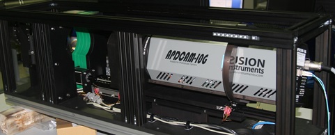
|
Figure. 2. An APDCAM-10G camera in direct imaging setup (left) and fibre head for coupling light with 1.3 mm fused silica fibres into an APDCAM (right). |